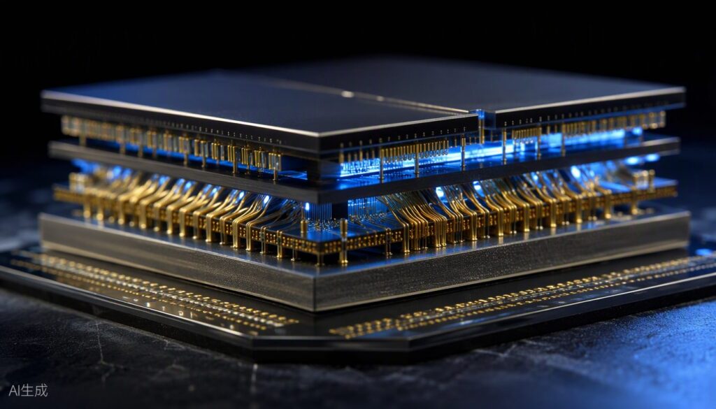
The RK1828, first product of Rockchip’s RK182X family announced in 2025 and in volume production in 2026, is a dedicated accelerator for on-device LLM inference. Paired with host SoCs such as the RK3588 and RK3576, it forms a “host plus AI co-processor” heterogeneous dual-chip design connected through standard interfaces such as PCIe.
Key specifications: the NPU delivers 20 TOPS of INT8 compute with mixed-precision support and deep optimization for Transformer architectures. The chip adopts a 3D-stacked memory design integrating 5 GB of high-bandwidth DRAM — among the first mass-produced 3D-stacked edge devices in the industry — targeting the “memory wall” of LLM inference and substantially reducing latency.
In application, the RK1828 runs 2B-7B-parameter LLMs and multimodal models smoothly on-device, with typical scenarios including smart cockpits, industrial edge boxes, smart home and robotics. The next generation is also planned to support multi-chip cascading, extending parameter scale to the tens of billions.
For device makers, the co-processor route means an AI upgrade does not require a board redesign: existing RK3588/RK3576 mainboard designs can gain on-device LLM capability simply by adding an RK1828 — a particularly friendly path for retrofitting installed products.
Sources: Rockchip official news, compiled from public materials